.png)
WCLSG: Electrical Engineering & PCB Design
(This project listing describes the electrical engineering & PCB design progress, considerations, and lessons learned from the Wirelessly-Connected Laser Shooting Gallery Project)
As one of the two Computer Engineering students on our project team, it initially wasn't my primary responsibility to handle electrical and PCB design work for the project. However, as the semester progressed and other responsibilities took hold of our primary EE student, I ultimately stepped up to design all three versions of all of our primary PCBs, and made some electrical design decisions along the way. Here's what we did, and what I learned.
What did we need?
Our system is a "Wirelessly Connected Laser Shooting Gallery." We've defined that as a system with two primary hardware platforms, a "controller" and a "target." Each of these devices primarily holds an ESP32 microcontroller (selected for its wireless communication abilities, as well as for its ability to manage the wide array of peripherals), but also holds our power management, an audio DAC/amplifier chip, and a few extra peripherals for each platform. On the controller, we have an OLED display over SPI, a laser diode, and a trigger, while the targets each have an array of phototransistors and an array of WS2182 NeoPixel RGB LEDs. Each board needed, too, a programming header, extra buttons for development, a power switch, and more.
Ultimately, we tried to make both platforms as similar to each other as possible, sharing designs and parts as we could to minimize complexity and development time.
Power
As wireless devices, it's expected that these devices have a built-in battery supply, one that discharges to provide power during runtime, and some way to recharge the batteries with some sort of standard connector. This was one of the biggest challenges - and missed opportunities - of the project. We did include a battery on both devices, but we neglected to include any battery charging circuitry (or connections), relying on external battery charging hardware to return our devices to service after being drained. I'm sure we could have included one, if we put the time and effort in, but we had enough issues with our voltage regulators already...
Voltage Regulators
The batteries we were provided (by a company that employed one of our EE majors on the team) were large, high-capacity, but also relatively high-voltage at about 14.8V. Our microcontrollers, the ESP32, run at 3.3V, and the LEDs on the target run at 5V. We need to step this voltage down to usable levels, not to mention regulation, so, Voltage Regulators.
These were initially left to one of the EE students on the team - you can hear him discussing his thought process for our voltage regulators in the full presentation video on the main project page. We ultimately had issues with consistency on the ones we chose, and had to change to another at the last revision.
PCB V1
| Target | Controller |
 |
 |
The first revision of our PCBs were designed by me and another student at the same time, working side-by-side, with my responsibility being the Target PCB. We ordered these PCBs from JLCPCB in late January, with the knowledge that they would probably not work completely, hoping to learn more about the actual process of PCB design and some knowledge about improvements for later versions.
A few notes on the target's design:
- We used a level-shifter chip (SN74AHCT125N) in order to change between the 3.3V logic level of the ESP32 and the 5V logic level of the NeoPixel RGBs. This ultimately turned out to be unnecessary and was dropped by Rev3
- There's a 12V line on the target board at this point. This was used for the phototransistor, to ensure results large enough for the ESP32 to notice. This was ultimately dropped when we changed to a different part.
- The ESP32's footprint is tiny. We used the ESP32-mini package, initially, as it was the first ones we found in stock. However, we found them... difficult to work with. Footprints in genral were difficult throughout our process, and these boards contained one of the biggest footprint mistakes we made...
| Target | Controller |
 |
 |
Our voltage regulator footprints were totally incorrect.
Somewhere in the import process for that part, we messed up the scale big-time, causing the voltage regulator pads to be absolutely massive compared to the part itself. Our EE members managed to solder them on, somehow, but... it was messy. They really didn't work. Power was not being regulated consistently for any of our voltage lines.
The second biggest problem in this PCB was the ESP32s. We couldn't get any communication with them to work. No errors reported, no noise on the lines, even feeding them 3V directly caused nothing to work. We ultimately decided this was due to some issues with the assembly process - soldering an SMD microcontroller onto a board using a heat-gun wouldn't get enough solid, clean connections to make this work, at least not reliably. So, revision 2 was in order.
Before that, there was two more PCBs we designed and ordered - a "menu buttons" daughterboard, and a power-switch board. These boards were designed to be slotted in to the final controller, holding smaller passive devices like a power switch and two buttons. They're mostly unremarkable, but there was something interesting that happened with the menu-buttons board, so I'll share that here.
| Schematic | Assembled |
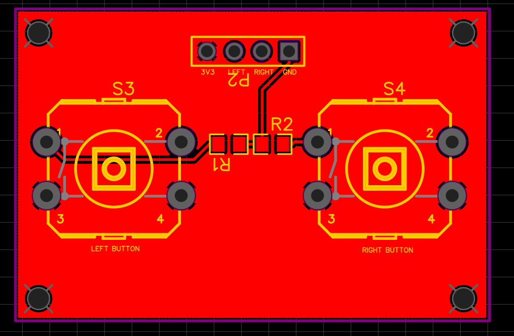 |
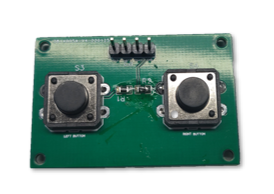 |
So, these buttons are designed to be active-low. When either button is pressed, their respective line (left/right) drops down to GND. When I first plugged them in, and began using them, however, I noted something... incorrect about their behavior. It was the opposite of what we expected. When pressed, they instead rose up to reach 3V3. In addition, there was also some weird behavior that both buttons would go low when one was pressed, leading to much confusion and attempts to debounce or limit the buttons in software.
Those of you more eagle-eyed might have spotted the issue already. After many weeks of living with this weird behavior, I finally took a look at it while in the lab. We re-assembled the board from scratch, tested each point, and took a break to get lunch. While eating, I took one final look at the board and finally realized what was wrong.
I'd marked the connection backwards.
3V3 was marked as ground, GND was marked as 3V3, and l/r were swapped.
This meant that we'd been dumping 3V3 into the ground plane of the board. When any button was pressed, that 3V3 would be shorted into the GND line (with a resistor), but this drop in voltage would cause the entire board to trigger every time a button was pressed.
It's always the simplest mistakes that trip you up the most.
Ultimately, we decided not to re-manufacture the board. We could just remember to ignore the silkscreen and attach things correctly, and we'd have no issues.
PCB V2
This was our final "proof of concept" order, with the hopes being that the next PCB round would be our final ones, the ones we use on the final assembly. Fixed the footprint issues, different MCU, some slight changes, a whole new layout on the controller board.
| Target | Controller |
 |
 |
This one worked! Mostly. Once again, we had some issues with it, but the Controller board worked perfectly once fully assembled. Voltage regulators were stable enough, we were able to communicate and program the MCU, and even got the audio and laser working! Great!
Target did not work! At least, not with the power anyway. We'd see instances where we'd have one or two regulators work, but never the 3V3 lines, and never at the same time. We could still talk with the MCU, as long as we powered it from our FTDI programmer, but we couldn't power the accessories without an external power supply running at the required voltage.
| Target | Controller |
 |
 |
We gave up on those voltage regulators at this point. These were fancy switching regulators that relied upon some line to determine their output voltage, which we couldn't achieve reliably enough with passives, AND they required another line to even turn on, a line which required the MCU to be on already. Catch-22.
We looked into some simple linear regulators, grabbed those. Looked at minimizing the boards as much as possible. Level-shifter? Gone. 12V line? Unnecessary with a different phototransistor. Lots of wasted space. Get rid of it. We had enough time to make our final PCBs, and probably one more, but we didn't want to rush it. Get our final boards here, get them built, and present.
The controller board, thankfully, worked well enough at this point that the other CpE and I could get to work on testing our software implementation, and I could get started on our final enclosure work. The target was sort-of made to work, and I could get testing done on that, too.
The last big problem we had noticed starting with this board was that our audio amp chip wasn't working on the target. It worked perfectly fine on the controller, which had the same electrical schematic and code, but something about the target just made it nonfunctional.
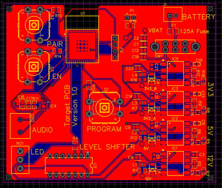
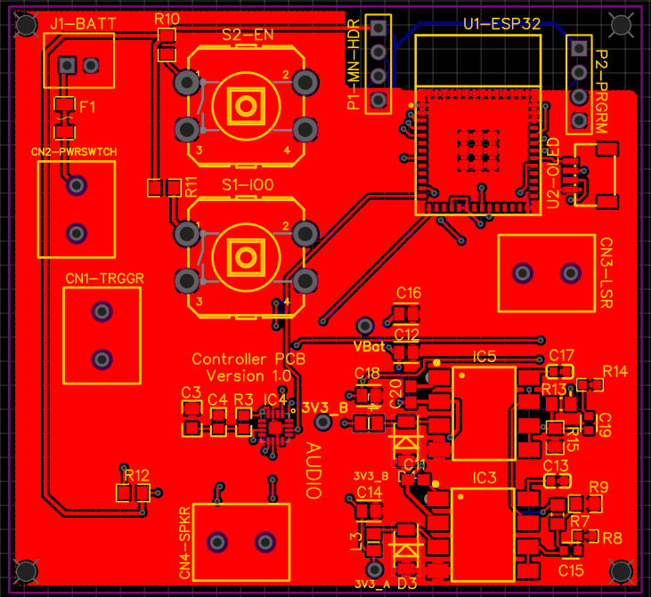
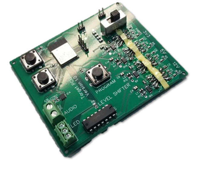
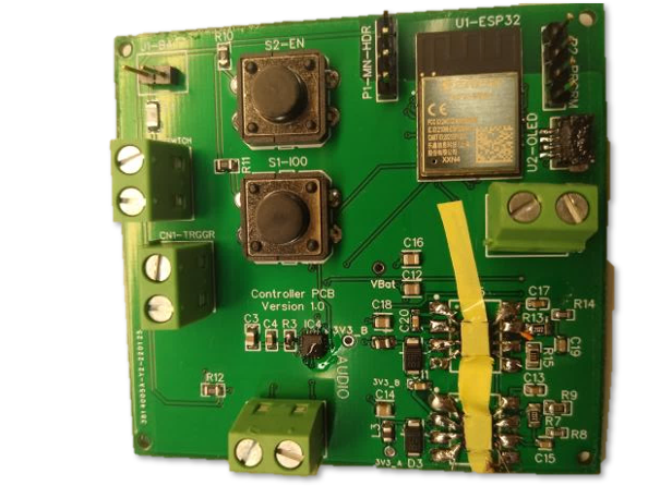
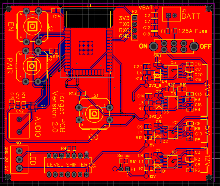
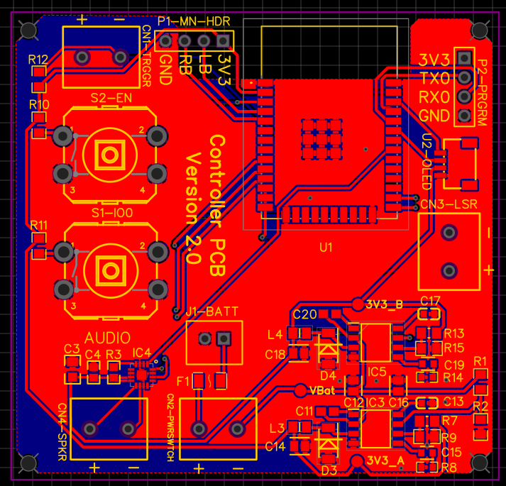
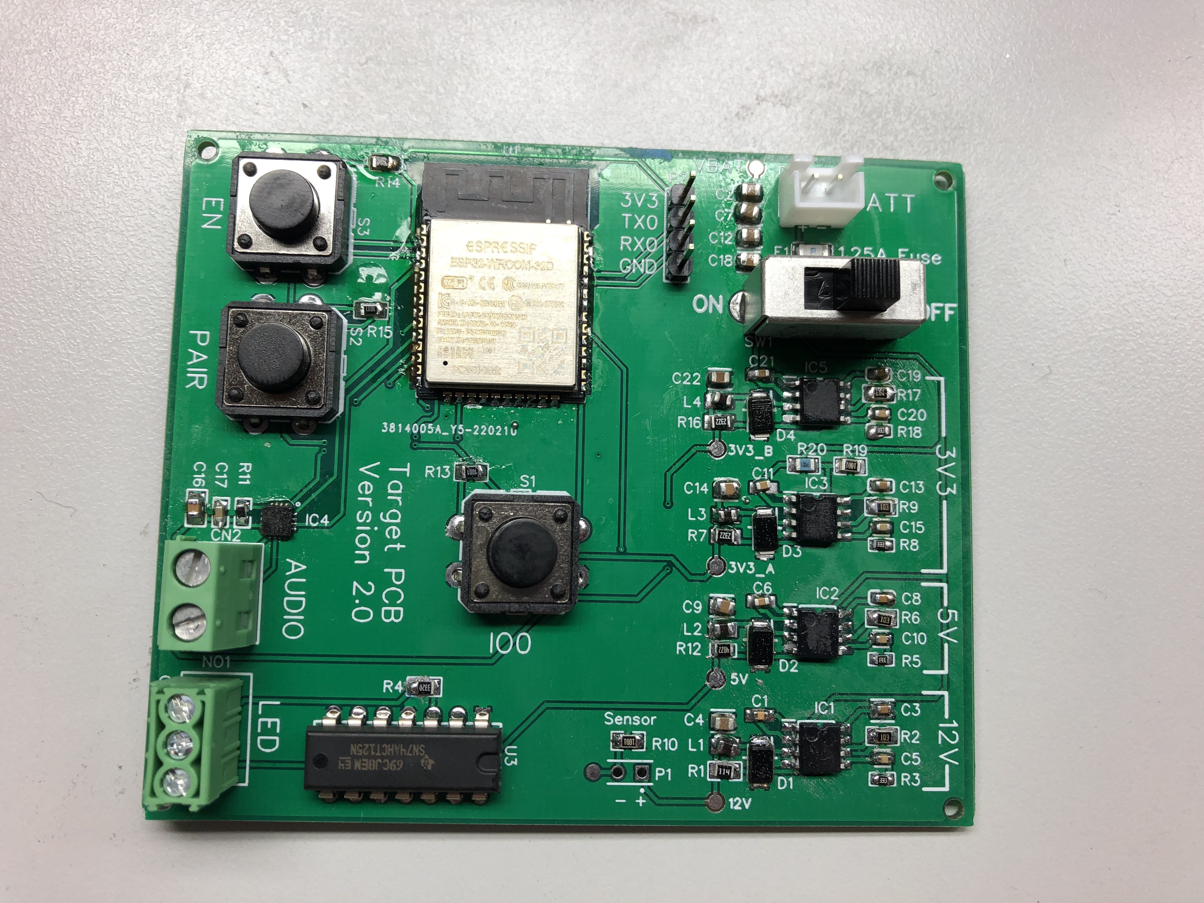
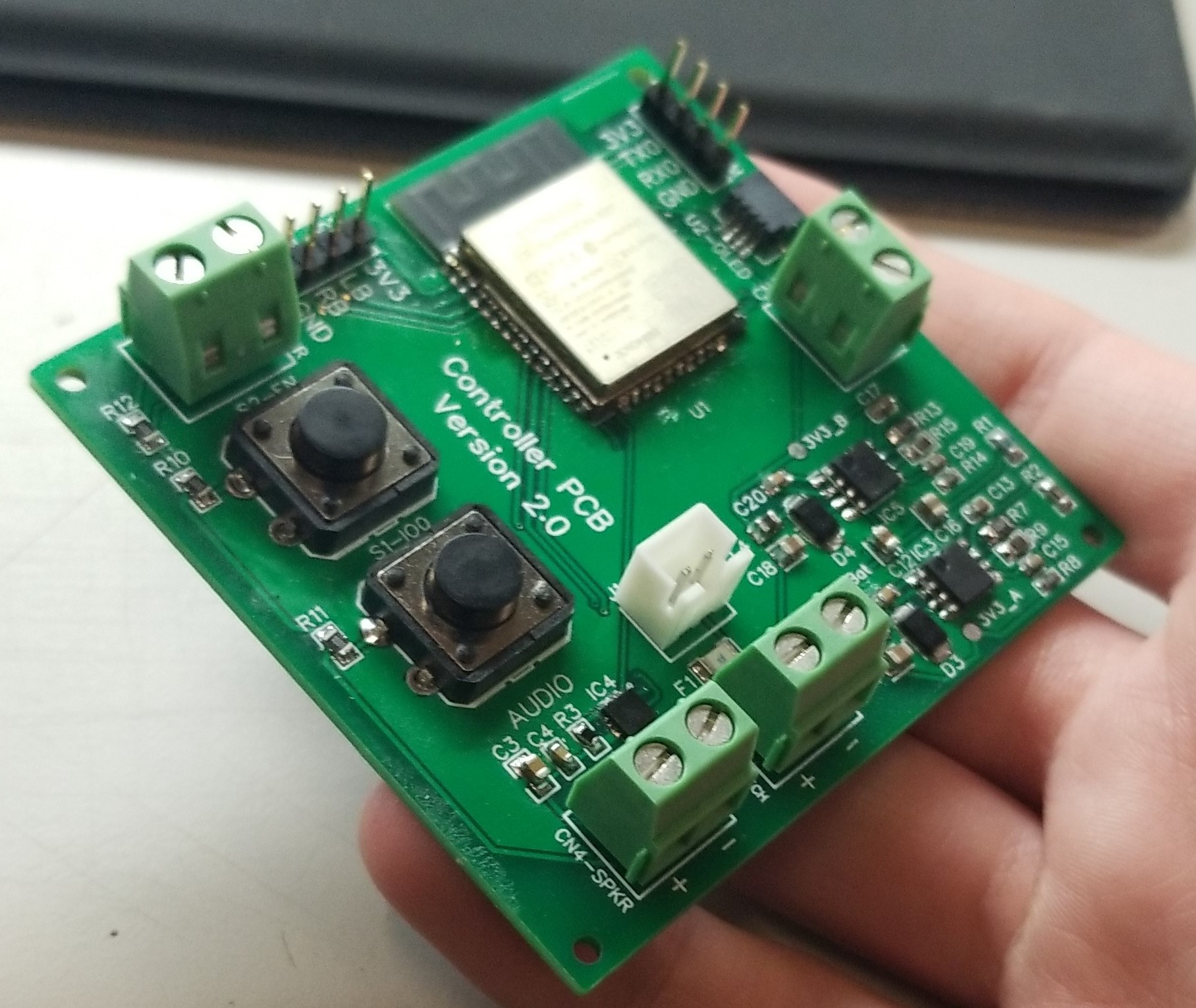
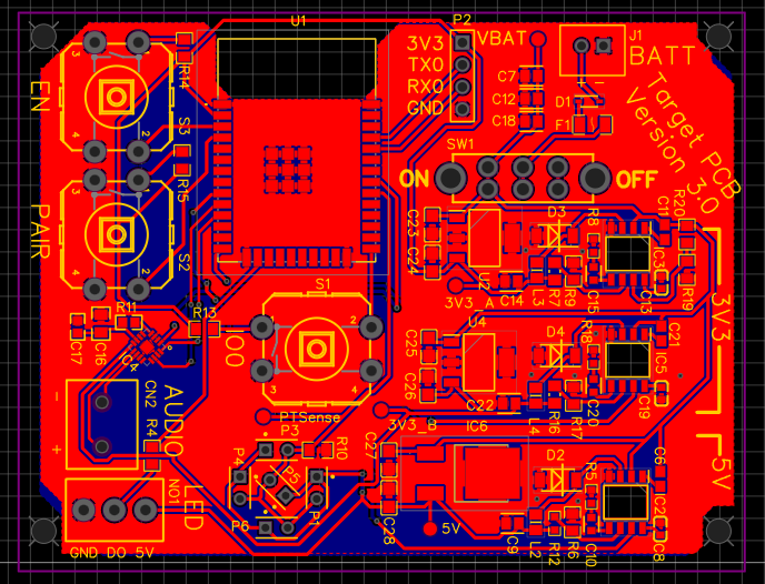
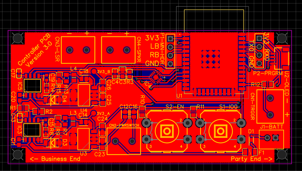
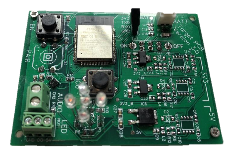
PCB V3
| Target | Controller |
 |
 |
An effort was taken to minimize these boards as much as possible, however, I didn't want to leave us totally reliant on these untested voltage regulators. As such, I stuck them in parallel with the old ones, with the thought being that we could utilize the old voltage regulators in a worst-case scenario, and leave them disconnected (or cut-off) if we didn't need them. Thankfully, we didn't, but they still took up space on the board we could've eliminated.
Another note - the big IO0/EN buttons. We should have removed them at this point, and slipped those lines into the programming header so our FTDI programmer could pull those high/low as required. However, I couldn't bring myself to remove them at this point. It'd worked. This was our final board. Without those lines in some way we'd have another dead board that couldn't do anything. So, I kept them in.
The phototransistors became an array on the target with this revision, too. Five sensors, all wired in parallel. 5V on one leg, current coming across the other leg being a measure of optical activity. Measure that across a simple resistor, and we had an easy voltage measurement for a larger area.
On shape: the controller board was intentionally made long, as to fit in the barrel of a laser pistol. Since I'd be responsible for the enclosure design, I knew that I'd be able to adjust the 3D printed enclosure much easier and cheaper than manufacturing a new PCB, so I decided to just minimize the boards as much as possible then design around them. You can read about how that turned out on the "Enclosure Design" page.
| Target | Controller |
 |
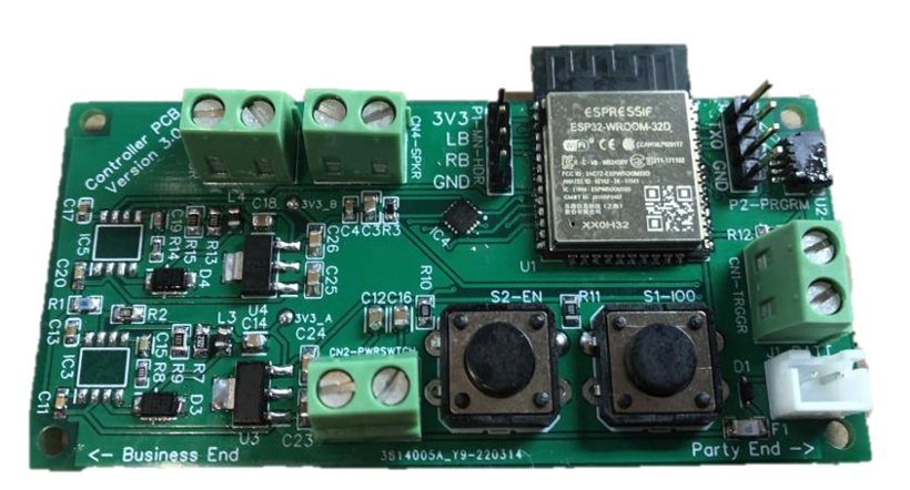 |
And they worked :D
Our new regulators worked (though they do get pretty crispy while running), all the peripherals on the controller worked, everything but the audio on the target worked (that subsystem was considered a lost cause at that point in the project).
You'll note that the "PAIR" and "ON/OFF" inputs on the target are actually mounted on the reverse side of the board. See the enclosure design for details there.
Lighting Array
Each target has on the front of their enclosures a set of 12 WS2182 NeoPixel RGB LEDs arranged in an "X" pattern. These LEDs are super convenient, control-wise: one line for power, another for ground, and then just a single data line that's daisy-chained across the whole system. You'll note that the target board has those three pins exposed via a screw terminal in the bottom left corner.
Wiring up the lights into their housing I designed and printed was easy, but repetitive, especially when we ultimately made three targets.
Unfortunately, we seem to have made some mistake at some point in the assembly process: one of our boards was unreliable when it came to lighting control. It'd work for a bit, but as the system ran for some time the data line became unstable and the lighting control failed to function properly, causing lights to change to apparently random colors or turn off, ignoring lighting commands. We didn't have the time to properly hunt down the source of this problem, but we did assemble a replacement lighting array, which proved that the problem was with the individual board.
Conclusion
Getting to design PCBs was an enlightening experience for me. I, personally, found it really interesting and peaceful to layout parts and routes, solving problems with routing on simple 2-layer PCBs. I wish we had done a bit more work to improve the overall electrical functionality of the device (try fix the audio/lighting problems on targets, include battery charging, change to a smaller form-factor battery), but I'm satisfied with what we ultimately made.
Thanks to our aggressive push for iteration as early as possible, we finished our electrical (and assembly) side of the project at least a week before the whole project was done, which was atypical compared to other groups in our academic class - some didn't even have a single PCB to present during the end of the semester. Proper scheduling and time management is important with hard-deadline projects like this.